|
|
|

I'm Online Chat Now
Certification
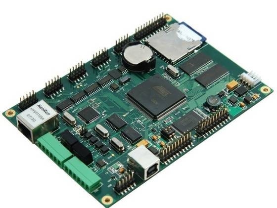
Multi Layer Printed Circuit Board Assemblies Prototype Quick Turn
|
Product Details:
Payment & Shipping Terms:
|

Detailed Product Description
| High Light: | electronic board assembly,SMD PCB Assembly |
||
|---|---|---|---|
Multi Layer Printed Circuit Board Assemblies Prototype Quick Turn
Characteristics:
1. Professional PCB manufacturer.
2. PCBA,OEM,ODM service are provided.
3. Gerber file needed.
4. Products are 100% E-tested.
5. Quality guarantee and professional after-sale service.
Details:
1. One of the largest and professional PCB (Printed Circuit Board) manufacturers in China with over 500 staff and 20 years’experience.
2. All kinds of surface finish is accepted,such as ENIG,OSP.Immersion Silver, Immersion Tin, Immersion Gold, Lead-free HASL,HAL.
3. BGA,Blind&Buried Via and Impedance Control is accepted.
4. Advanced production equipment imported from Japan and Germany,such as PCB Lamination Machine, CNC drilling machine,Auto-PTH line,AOI(Automatic Optic Inspection),Probe Flying Machine and so on.
5. Certifications of ISO9001:2008,UL,CE,ROHS,REACH,HALOGEN-FREE is meet.
6. One of the professional SMT/BGA/DIP/PCB Assembly manufacturers in China with 20 years’experience.
7. High speed advanced SMT lines to reach chip +0.1mm on integrated circuit parts.
8. All kinds of integrated circuits is available,such as SO, SOP, SOJ, TSOP, TSSOP, QFP, BGA and U-BGA.
9. Also available for 0201 chip placement, through-hole components insertion and finished products fabrication, testing and package.
10. SMD assembly and through-hole components insertion is accepted.
11. IC preprogramming is also accepted.
12. Available for Function verification and burn in testing.
13. Service for complete unit assembly,for example,plastics, metal box, coil, cable inside .
14. Environmental conformal coating to protect finished PCBA products.
15. Providing Engineering service as end of life components, obsolete component replace and design support for circuit, metal and plastic enclosure.
16. Functional testing,repairs and inspection of the sub-finished and finished goods.
17. High mixed with low volume order is welcomed.
18. Products before delivery should be full quality checked, striving to 100% perfect.
19. One-stop service of PCB and SMT(PCB assembly) is supplied to our customers.
20. Best service with punctual delivery is always provided for our customers.
|
Key Specifications/Special Features |
|
|
1 |
We SYF have 6 PCB production lines and 4 advanced SMT lines with high speed. |
|
2 |
All kinds of integrated circuits are accepted,such as SO, SOP, SOJ, TSOP, TSSOP, QFP, DIP, CSP,BGA and U-BGA , Because Our placement precision can reach chip +0.1mm on integrated circuit parts. |
|
3 |
We SYF can provide service of 0201 chip placement, through-hole components insertion and finished products fabrication, testing and packaging. |
|
4 |
SMT/SMD assembly and through-hole components insertion |
|
5 |
IC preprogramming |
|
6 |
Function verification and burn in testing |
|
7 |
Complete unit assembly (which including plastics, metal box, coil, cable inside and more) |
|
8 |
Environmental coating |
|
9 |
Engineering including end of life components, obsolete component replace and design support for circuit, metal and plastic enclosure |
|
10 |
Packaging design and production of customized PCBA |
|
11 |
100% quality assurance |
|
12 |
High mixed, low volume order is also welcomed. |
|
13 |
Full component procurement or the substitute components sourcing |
|
14 |
UL,ISO9001:2008, ROSH ,REACH,SGS,HALOGEN-FREE compliant |
|
PRODUCTION CAPABILITY OF PCB ASSEMBLY |
||
|
Stencil Size Range |
756 mm x 756 mm |
|
|
Min. IC Pitch |
0.30 mm |
|
|
Max. PCB Size |
560 mm x 650 mm |
|
|
Min. PCB Thickness |
0.30 mm |
|
|
Min. Chip Size |
0201 (0.6 mm X 0.3 mm) |
|
|
Max. BGA Size |
74 mm X 74 mm |
|
|
BGA Ball Pitch |
1.00 mm (Min) / F3.00 mm (Max) |
|
|
BGA Ball Diameter |
0.40 mm (Min) /F1.00 mm (Max) |
|
|
QFP Lead Pitch |
0.38 mm (Min) /F2.54 mm (Max) |
|
|
Frequency of Stencil Cleaning |
1 time / 5 ~ 10 Pieces |
|
|
Type of Assembly |
SMT and Thru-hole |
|
|
Solder Type |
Water Soluble Solder Paste,Leaded and Lead-free |
|
|
Type of Service |
Turn-key,Partial Turn-key or consignment |
|
|
File Formats |
Bill of Materials(BOM) |
|
|
Gerber Files |
||
|
Pick-N-Places(XYRS) |
||
|
Components |
Passive Down to 0201 Size |
|
|
BGA and VF BGA |
||
|
Leadless Chip Carries/CSP |
||
|
Double Sided SMT Assembly |
||
|
BGA Repair and Reball |
||
|
Part Removal and Replacement |
||
|
Component Packaging |
Cut Tape,Tube,Reels,Loose Parts |
|
|
Testing Method |
X-RAY Inspection and AOI Test |
|
|
Order of Quantity |
High Mixed,Low Volume Order is also welcomed |
|
|
Remarks: In order to get accurate quote,the following information is required |
||
|
1 |
Complete Data of Gerber Files for the Bare PCB Board. |
|
|
2 |
Electronic Bill of Material(BOM) / Parts list detailing manufacturer's part number, quantity usage of components for reference. |
|
|
3 |
Please state whether we can use alternative parts for passive components or not. |
|
|
4 |
Assembly Drawings. |
|
|
5 |
Functional Test Time Per Board. |
|
|
6 |
Quality Standards Required |
|
|
7 |
Send Us Samples (if available) |
|
|
8 |
Date of the quote needs to be submitted |
|
|
Note Book fields |
CHARGER BOARD |
INVERTER |
POWER CPU |
LVDS CARD |
IR BOARD |
|
LCD MOTHERBOARD |
LED BOARD |
RAM CARD |
DATA BOARD |
BATT BOARD |
|
|
DVR MOTHERBOARD |
USB BOARD |
CARD READER |
AUDIO BOARD |
ISDN MODEN |
|
|
PC fields |
2.5 inch HDD |
PC/MAC FDD |
DOCKING |
PORT REPILICATOR |
PCMCIA CARD |
|
3.5 inch HDD |
SATA HDD |
ADAPTER |
DVD ROM |
SSD |
|
|
Telecom fields |
DVBT.ATSC TV |
GPS UNIT |
CAR GPS UNIT |
ADSL MODEN |
3.5inch DVB-T RECEIVER |
|
Audio & Video fields |
MPEG 4 PLAYER |
KVM SWITCH |
E-BOOK READER |
HDMI BOX |
DVI BOX |
|
Electronic Security fields |
LCD TV MOTHERBOARD |
DVR MOTHERBOARD |
CCD BOARD |
IP CAMERA |
CCTV CAMERA |
|
Health & Medical fields |
DIGITAL TEMS UNIT |
EAR THERMOMETER |
BLOOD GLUCOSE TEST METERS |
BODY FAT MONITOR |
DIGITAL BLOOD PRESSURE MONITOR |
|
LED Application fields |
LED AUTO LAMP |
LED ROPE LIGHT |
LED BULB |
OUTDOOR LED DISPLAY |
PROJECTION LIGHTING |
|
Test Instrument fields |
OSCILLOSCOPE |
POWER SUPPLY |
L.C.R. METER |
LOGIC ANALYZER |
MULTIMETER |
|
Consumer Electronics fields |
SENSORS BOARD |
DRIVER BOARD |
USB DVIVER BOARD |
BAR-CODE PRINTER |
MP3 PLAYER |
|
SOLAR PANEL MODULE |
PEN TABLET |
USB HUB |
USB CARD READER |
USB FLASH DRIVE |
|
PRODUCTION CAPABILITY OF PCB |
||
|
|
ITEMS Item |
|
|
Laminate |
Type |
FR-1,FR-5,FR-4 High-Tg,ROGERS,ISOLA,ITEQ, |
|
Thickness |
0.2~3.2mm |
|
|
Production Type |
Layer Count |
2L-16L |
|
Surface Treatment |
HAL,Gold Plating,Immersion Gold,OSP, |
|
|
Cut Lamination |
Max. Working Panel size |
1000×1200mm |
|
Inner Layer |
Internal Core Thickness |
0.1~2.0mm |
|
Internal width/spacing |
Min: 4/4mil |
|
|
Internal Copper Thickness |
1.0~3.0oz |
|
|
Dimension |
Board Thickness Tolerance |
±10% |
|
Interlayer Alignment |
±3mil |
|
|
Drilling |
Manufacture Panel Size |
Max: 650×560mm |
|
Drilling Diameter |
≧0.25mm |
|
|
Hole Diameter Tolerance |
±0.05mm |
|
|
Hole Position Tolerance |
±0.076mm |
|
|
Min.Annular Ring |
0.05mm |
|
|
PTH+Panel Plating |
Hole Wall copper Thickness |
≧20um |
|
Uniformity |
≧90% |
|
|
Outer Layer |
Track Width |
Min: 0.08mm |
|
Track Spacing |
Min: 0.08mm |
|
|
Pattern Plating |
Finished Copper Thickness |
1oz~3oz |
|
EING/Flash Gold |
Nickel Thickness |
2.5um~5.0um |
|
Gold Thickness |
0.03~0.05um |
|
|
Solder Mask |
Thickness |
15~35um |
|
Solder Mask Bridge |
3mil |
|
|
Legend |
Line width/Line spacing |
6/6mil |
|
Gold Finger |
Nickel Thickness |
≧120u〞 |
|
Gold Thickness |
1~50u〞 |
|
|
Hot Air Level |
Tin Thickness |
100~300u〞 |
|
Routing |
Tolerance of Dimension |
±0.1mm |
|
Slot Size |
Min:0.4mm |
|
|
Cutter Diameter |
0.8~2.4mm |
|
|
Punching |
Outline Tolerance |
±0.1mm |
|
Slot Size |
Min:0.5mm |
|
|
V-CUT |
V-CUT Dimension |
Min:60mm |
|
Angle |
15°30°45° |
|
|
Remain Thickness Tolerance |
±0.1mm |
|
|
Beveling |
Beveling Dimension |
30~300mm |
|
Test |
Testing Voltage |
250V |
|
Max.Dimension |
540×400mm |
|
|
Impedance Control |
|
±10% |
|
Aspect Ration |
12:1 |
|
|
Laser Drilling Size |
4mil(0.1mm) |
|
|
Special Requirements |
Buried And Blind Via, Impedance Control, Via Plug, |
|
|
OEM&ODM Service |
Yes |
|
Contact Details
China Card Reader Online Market
Tel: +86-755-26710992
Send your inquiry directly to us